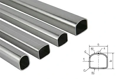
Within Chalco's broader semiconductor sputtering target materials range, copper and copper alloy sputtering targets are primarily used to form copper interconnects, seed layers, and copper-based functional thin films in semiconductor PVD processes. High-purity copper targets are suitable for UBM, TSV, TGV, and RDL applications, while CuMn targets serve applications requiring stricter control over alloy composition and microstructural uniformity.
We supply high-purity copper and CuMn sputtering targets, backed by full in-house manufacturing capabilities-from ultra-high-purity copper refining and alloy melting to grain and crystallographic orientation control, precision machining, target bonding, automated cleaning, vacuum packaging, and quality inspection. Products can be customized as monolithic or backing-plate-bonded structures based on tool type, chamber design, and existing target drawings. We support control over dimensions, critical impurities, alloy ratios, surface quality, and bond integrity to enable direct replacement, sample validation, and second-source qualification.
Copper and Copper Alloy Sputtering Target Products
We offer high-purity copper sputtering targets and CuMn copper-manganese alloy sputtering targets for semiconductor PVD applications. Specifications are matched to film design, tool architecture, target dimensions, microstructure, and bonding method, supporting monolithic, bonded, or custom-engineered configurations.
High-Purity Copper Sputtering Targets
High-purity copper sputtering targets are primarily used in semiconductor copper interconnects, UBM, TSV, TGV, RDL, and wafer-level packaging metallization processes. Key controls include material purity, oxygen and metallic impurities, grain structure, internal defects, and surface cleanliness to ensure stable copper film deposition and batch consistency.

| Specifications | Available Range |
| Material | High-purity copper |
| Purity | 6N, ≥99.9999% |
| Common Sizes | 6-inch, 8-inch, 12-inch |
| Product Structure | Monolithic or backing-plate bonded |
| Grain Structure and Crystallographic Orientation | Controlled according to target grade and process requirements |
| Surface Condition | Precision machining, cleaning, and vacuum packaging |
| Bonding Method | FSW, DB, HIP, or evaluated based on structure |
| Key Inspections | Composition and impurities, LECO, EBSD, C-Scan, dimensional and surface inspection |
| Customization Options | Diameter, thickness, edge profile, hole positions, backing plate, and mounting features |
CuMn Copper-Manganese Alloy Sputtering Targets
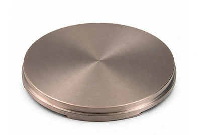
CuMn copper-manganese sputtering targets use high-purity copper as the base material, with controlled manganese content and microstructure to meet stringent requirements for copper-based alloy films, compositional uniformity, and process stability in semiconductor PVD applications. Mn content, impurity limits, grain structure, and target configuration can be confirmed against existing process specifications.
| Specifications | Available Range |
| Material | CuMn copper-manganese alloy |
| Base Material | High-purity copper |
| Base Purity | 6N grade, subject to formal specification confirmation |
| Mn Content | Confirmed based on film and process requirements |
| Alloy Composition | Cu–Mn |
| Dimensions | Confirmed based on tool, chamber, and target drawings |
| Alloy Uniformity | Controlled distribution of composition across surface and bulk |
| Grain Structure and Crystallographic Orientation | Confirmed according to CuMn target grade |
| Product Structure | Monolithic or backing-plate bonded |
| Surface Condition | Precision machining, cleaning, and vacuum packaging |
| Key Inspections | Alloy composition, critical impurities, EBSD, C-Scan, and dimensional inspection |
Target Dimensions and Structural Configuration
We supply 6-inch, 8-inch, and 12-inch high-purity copper targets and develop CuMn targets per project specifications. Outer diameter, thickness, edge profile, backing plate, rear-side features, and mounting interfaces can be customized based on PVD tool, chamber, and cathode design, supporting monolithic, bonded, or drawing-based manufacturing solutions.
Target Form: Circular planar targets and custom shapes per drawing
Key Dimensions: Outer diameter, thickness, and assembly height confirmed per tool drawings
Product Structure: Monolithic or backing-plate bonded
Backing Plate Configuration: Material, dimensions, and cooling-side features confirmed per project
Machined Features: Steps, grooves, center holes, mounting holes, and alignment features
Surface and Tolerances: Surface roughness, flatness, and dimensional tolerances executed per approved drawings
-
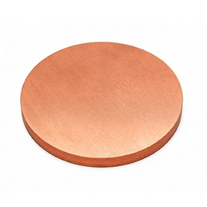 Circular Planar Copper Sputtering Target
The circular planar target is a common configuration in semiconductor wafer PVD. Actual diameter, thickness, and edge geometry must be confirmed based on tool interface requirements.
-
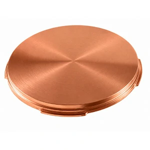 Monolithic Copper Sputtering Target
The target body uses a monolithic structure without an interface between the sputtering layer and a dissimilar backing plate.
-
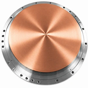 Monolithic Copper Sputtering Target
The target is integrated with an aluminum, copper, or other backing plate into a complete assembly. The backing plate and bonding method are selected based on thermal management, power density, and cathode design.
-
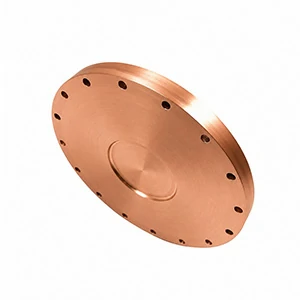 Custom Machined Copper Sputtering Target
Supports custom machining of steps, grooves, mounting holes, alignment features, and specialized rear or edge profiles for direct replacement and tool compatibility.
Semiconductor Copper Target Application Solutions
For various semiconductor PVD and advanced packaging processes, we provide high-purity copper or CuMn target selection, structural matching, sample validation, and volume ramp-up support based on film design, tool model, chamber architecture, and existing target specifications. For package-level electrical interconnects outside the PVD deposition step, Chalco also supplies die-to-package bonding materials, including semiconductor bonding wire and semiconductor bonding ribbon.
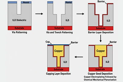
Copper Interconnect Seed Layer
Material Control:High-purity copper with low impurities
Process Matching:Optimized target grade and structure
Qualification Support:From sample validation to volume supply

UBM and Wafer-Level Packaging
Structural Compatibility:Tool and backing plate adaptation
Batch Control:Consistent material and machining quality
Replacement Development:Second-source qualification support
TSV, TGV, and RDL
Target Customization:Monolithic or bonded options
Tool Compatibility:Dimension and interface matching
Project Support:From prototyping and validation to volume delivery
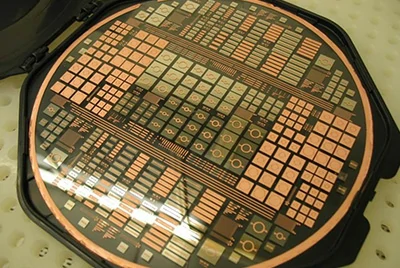
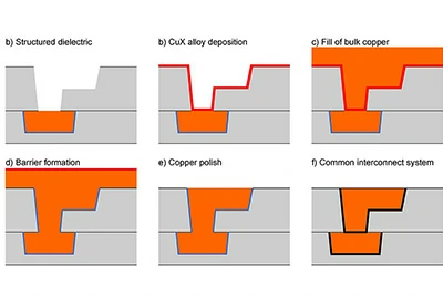
Advanced Copper Alloy Metallization
Composition Customization:Mn content tailored to requirements
Microstructure Control:Enhanced alloy and grain uniformity
Process Validation:Specification adjustment and testing support
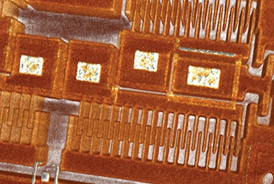
Power Semiconductors and MEMS
Flexible Customization:Non-standard specifications supported
Drawing-Based Machining:Profile and backing plate matching
Phased Qualification:Samples, pilot lots, and mass production
How to Choose Between High-Purity Copper and CuMn Targets
High-purity copper and CuMn copper-manganese sputtering targets serve different film designs and semiconductor PVD processes. Selection should be based on target film composition, alloy requirements, tool architecture, critical impurities, and approved process specifications-not solely on purity or price.
| Selection Criteria | High-Purity Copper Target | CuMn Copper-Manganese Target |
| Material System | High-purity copper | High-purity copper-based Cu-Mn alloy |
| Application Focus | General semiconductor copper metallization | Specialized copper alloy metallization processes |
| Typical Applications | Copper interconnects, UBM, TSV, TGV, RDL | Copper alloy seed layers and functional thin films |
| Key Controls | Purity, critical impurities, grain structure, and particle performance | Mn content, compositional uniformity, impurities, and grain structure |
| Specification Confirmation | Match existing specs or develop standard projects | Customized based on film composition and process requirements |
| Validation Focus | Chamber compatibility, film stability, and batch consistency | Composition, microstructure, and process validation |
High-purity copper targets are better suited for broad copper seed layer and conductive metallization applications, while CuMn targets are ideal for projects with defined requirements for Mn content and copper-based alloy films. Final material selection should be based on target film composition, alloy ratio, PVD chamber design, and approved process specifications. For semiconductor projects based on an aluminum target system rather than Cu or CuMn, aluminum and aluminum alloy sputtering targets should be evaluated as a separate material route.
Material and Manufacturing Advantages
Ultra-High-Purity Raw Material Base: Capable of producing 7N and 8N ultra-high-purity copper feedstock; finished copper targets available in 6N grade.
CuMn Composition Control: Mn content, alloy uniformity, and grain structure tailored to process requirements.
Integrated Finished Product Supply: Supports precision machining, monolithic or bonded structures, cleaning, inspection, and vacuum packaging.
Production Capacity and Quality Control
We provide end-to-end manufacturing support-from high-purity copper feedstock and CuMn alloy melting to grain control, CNC machining, target bonding, cleaning, packaging, and final inspection-and collaborate with customers on sample validation and second-source qualification.
High-Purity Feedstock: Capable of 7N and 8N ultra-high-purity copper; finished copper targets offered in 6N grade.
Alloy and Microstructure: Supports control of CuMn composition, grain structure, and microstructural uniformity.
Finished Product Manufacturing: Supports monolithic targets and FSW/DB bonded configurations with precision CNC machining.
Clean Processing: Automated cleaning, clean drying, and vacuum packaging provided.
| Inspection Items | Control Methods |
| Purity and Metallic Impurities | GDMS or ICP-MS |
| CuMn Alloy Composition | Composition and uniformity analysis |
| Light Elements (O, C, etc.) | LECO analysis |
| Grain Structure and Crystallographic Orientation | EBSD or metallographic inspection |
| Internal and Bonding Defects | C-Scan Inspection |
| Dimensions and Tolerances | CMM Precision Measurement |
| Surface Quality | Roughness, Flatness, and Cleanliness Inspection |
Based on your existing part numbers, drawings, legacy targets, and tool configurations, we offer: prototype target fabrication, material and structural matching, post-PVD specification adjustments, second-source validation, and volume supply after sample approval. Sample inquiries are welcome.

FAQ
1. What is copper sputtering target primarily used for in semiconductor manufacturing?
High-purity copper sputtering targets are primarily used in PVD metallization processes for copper interconnect seed layers, UBM, TSV, TGV, RDL, and wafer-level packaging. The specific target grade and structure must be confirmed based on film stack design, tool type, and chamber configuration.
2. What is the difference between high-purity copper targets and CuMn targets?
High-purity copper targets are suitable for a wide range of copper conductive and seed layer depositions, with emphasis on purity, impurity control, grain structure, and particle performance. CuMn targets are used for specific copper alloy films and require tighter control over Mn content, alloy homogeneity, and microstructure.
3. Can the Mn content in CuMn targets be customized?
We can evaluate the Mn content and allowable tolerance based on your film composition, existing process specifications, and qualification requirements. Once samples are approved, the material composition and volume production parameters can be finalized.
4. Do you supply 6-inch, 8-inch, and 12-inch copper targets?
High-purity copper targets are available in 6-inch, 8-inch, and 12-inch sizes. CuMn target dimensions depend on product specifications and project requirements. Actual outer diameter, thickness, edge profile, and backing plate design should always be confirmed against tool drawings.
5. What is the difference between monolithic and bonded targets?
Monolithic targets are machined directly from a single piece of target material without an interface to a dissimilar backing plate. Bonded targets consist of a target bonded to a backing plate, allowing selection of bonding solutions based on thermal management, power handling, cathode interface, and mechanical assembly requirements.
6. Can you produce replacement targets based on existing drawings or legacy targets?
We can evaluate material, dimensions, profile, and backing plate structure based on your existing target drawings, part numbers, photos, or physical samples, and support prototyping, PVD validation, and second-source qualification.
Submit Copper Target Drawings and Process Requirements
Based on your existing drawings, target samples, PVD tool type, and process specifications, we can assess high-purity copper or CuMn target solutions and support you from specification confirmation and prototyping through process validation to volume ramp-up.
When requesting a quote, please provide:
- Target material: high-purity copper or CuMn
- Purity grade or Mn content
- Target diameter and thickness
- Tool and chamber model
- Monolithic or bonded construction
- Backing plate drawing and assembly requirements
- Grain size and critical impurity specifications
- Existing part number, drawing, or photo of legacy target
- Sample quantity and estimated annual usage
Send your current target specifications or tool drawings to receive a tailored solution for material, structure, and sample validation.
Chalco can provide you the most comprehensive inventory of aluminum products and can also supply you customized products. Precise quotation will be provided within 24 hours.
Get a quote