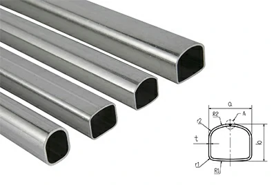
High purity copper refers to copper material with extremely low impurity content, typically including 5N, 6N, 7N, and even higher purity grades. Compared to standard copper, high purity copper offers superior purity, better electrical conductivity, lower residual impurities, and more consistent batch-to-batch performance, making it suitable for applications in semiconductors, electronics, vacuum deposition, and advanced scientific research.
Chalco supplies 5N, 6N, 7N, and project-based 8N high purity copper. Our primary products include high purity copper sheets, strips, ingots, target blanks, and sputtering targets, supporting Chalco's broader semiconductor sputtering target materials range as well as integrated circuit and advanced electronic material applications.
High purity copper grades
Chalco can supply 5N, 6N, 7N, and project-based 8N high purity copper according to different application requirements. These purity levels match various use cases such as electronic materials, semiconductor sputtering targets, vacuum coating, cryogenic research, and high-purity alloy feedstock.
| Purity grade | Copper purity | Typical products | Typical applications |
| 5N copper | 99.999% | High purity copper sheet, strip, ingot, and rod | Electronic materials, evaporation coating materials, display coating, and research materials |
| 6N copper | 99.9999% | High purity copper sheet, ingot, target blank, and Cu target | Semiconductor sputtering targets, IC materials, PVD coating |
| 7N copper | 99.99999% | 7N copper sheet, 7N copper strip, target blank | Advanced semiconductor sputtering targets, advanced electronic materials, thin-film deposition materials |
| 8N copper | 99.999999% | Project-based ultra-high purity copper material | Cryogenic research, superconducting materials, quantum research, specialized semiconductor projects |
High purity copper products
Chalco offers a variety of high purity copper product forms, covering high purity raw materials, target blanks, copper and copper alloy sputtering targets, and vacuum deposition materials. Products can be customized based on purity grade, dimensions, form, surface condition, and testing requirements.
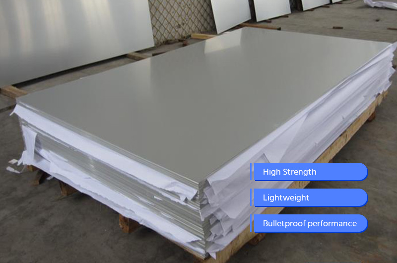
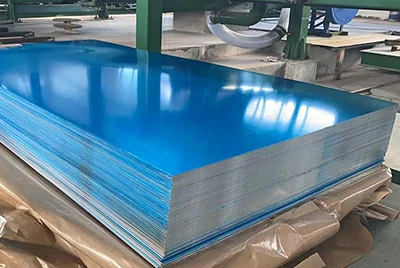
High purity copper sheet
Grade:5N, 6N, 7N, 8N
Dimensions:thickness 0.1–50 mm
Applications:semiconductor target blanks, electronic materials, precision machined components, thin-film deposition materials

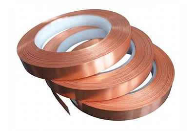
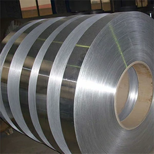
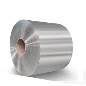
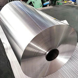
High purity copper strip
Grade:5N, 6N, 7N
Dimensions:thickness 0.01–3 mm, width 5–300 mm; available in coil or cut-to-length form
Applications:electronic materials, display coating, vacuum deposition materials, high purity machining materials
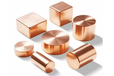
High purity copper ingots
Grade:5N, 6N, 7N, project-based 8N
Dimensions:diameter Φ20–Φ400 mm; weight and shape customizable
Applications:remelting, high purity alloy feedstock, copper target blank production, semiconductor material preparation
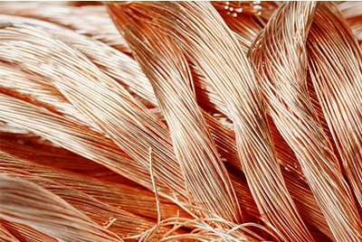
High purity copper wire
Grade:5N, 6N, project-based 7N / 8N
Dimensions:diameter Φ0.01–3 mm; spool length and packaging customizable
Applications:electronic materials, cryogenic systems, superconducting equipment, research materials
Copper sputtering targets
Grade:High purity Cu, CuMn, Cu alloy
Dimensions:2–12 inch, thickness 3–20 mm; available as planar targets, bonded targets, or custom configurations
Applications:Semiconductor PVD, integrated circuits, copper interconnects, display coating, Micro OLED
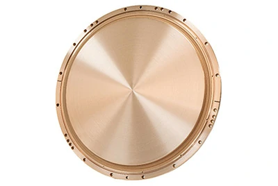
Features of high purity copper
High purity copper exhibits high electrical conductivity, excellent thermal conductivity, good ductility, and stable chemical properties, making it suitable for semiconductor sputtering targets, electronic materials, bonding wires, vacuum deposition, thermal management, and high purity alloy feedstock. For package-level interconnect requirements beyond the high-purity-copper material route, Chalco also supplies die-to-package bonding materials, including semiconductor bonding wire and semiconductor bonding ribbon.
- High electrical conductivity: High purity copper typically achieves electrical conductivity exceeding 100% IACS, with some oxygen-free copper reaching ≥101.5% IACS-ideal for cables, busbars, electronic connectors, and semiconductor-related materials.
- Excellent thermal conductivity: High purity copper has a thermal conductivity of approximately 393–401 W/(m·K), suitable for heat sinks, heat exchangers, electronic thermal management components, and high-conductivity precision parts.
- Good ductility and workability: High purity copper offers excellent plasticity and ductility, enabling rolling, drawing, bending, stamping, forging, and precision machining-ideal for producing copper foil, wire, strip, sheet, and target blanks.
- Low impurity content: Impurities such as Fe, Si, Ag, S, Cl, O, and C can be tightly controlled to minimize their impact on electrical conductivity, thermal conductivity, ductility, and material stability.
- Uniform microstructure: Dense internal structure with homogeneous grain distribution and minimal intermetallic inclusions-suitable for semiconductor copper sputtering targets, target blanks, evaporation coating materials, and high purity electronic materials.
- Corrosion resistance: High purity copper demonstrates good corrosion resistance in atmospheric conditions, fresh water, certain seawater environments, and non-oxidizing acids-ideal for electronics, power systems, marine engineering, and long-term stable applications.
- Chemical stability: High purity copper remains stable in normal atmospheric conditions, fresh water, and most non-strongly oxidizing environments; however, it is not suitable for prolonged exposure to nitric acid, hot concentrated sulfuric acid, or strongly corrosive ammonia-based media.
- Superior surface quality: Oxidation, oil contamination, scratches, and particle residues can be minimized through cleaning, drying, and clean packaging-making it suitable for copper sputtering targets, evaporation materials, and precision electronic applications.
Key applications of high purity copper
Applications in the semiconductor industry
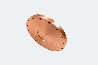
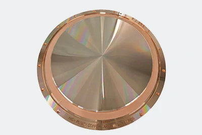
Semiconductor sputtering targets
High purity copper is used in copper sputtering targets, CuMn targets, and copper target blanks, suitable for copper interconnects, seed layers, and physical vapor deposition (PVD) processes in chip manufacturing.
Integrated circuit materials
High purity copper serves as interconnect material, electronic connectors, and high purity conductive components in integrated circuits-ideal for precision electronic devices and high-reliability electrical connections.
Display and memory devices
High purity copper sputtering targets are used in the fabrication of liquid crystal displays, micro-OLEDs, information storage devices, laser memory, and other functional thin-film materials.

Advanced packaging materials
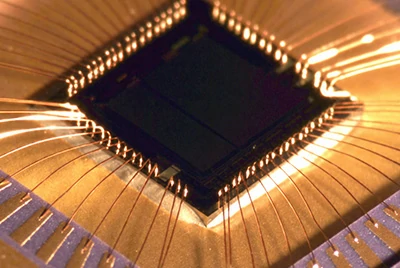
High purity copper is used in select advanced packaging interconnects, copper pillars, conductive structures, and high purity electronic materials-providing the foundation for electrical conduction and thermal management in packaging.
Applications in other fields
- High purity copper wire: Offering excellent electrical conductivity and ductility, it is used in electronic interconnects, high-fidelity audio cables, precision signal transmission lines, and certain cryogenic conductive materials.
- Vacuum evaporation coating materials: High purity copper granules, chunks, and evaporation sources are used in vacuum evaporation, optical coatings, sensor coatings, and research-grade deposition.
- New energy applications: High purity copper is used in electric vehicles, battery management systems, photovoltaic modules, wind power equipment, and high-efficiency current transmission components.
- Cryogenic superconductivity and research systems: 6N, 7N, and project-based 8N ultra-high purity copper are used in cryogenic research, superconducting devices, quantum research, and advanced experimental materials.
- Thermal management components: Thanks to its excellent thermal conductivity, high purity copper is used in heat sinks, heat exchangers, electronic thermal management parts, and high-conductivity precision components.
- High purity alloy feedstock: High purity copper serves as raw material for copper alloy ingots, advanced electronic alloys, research materials, and specialty functional materials.
Impurity control comparison in high purity copper
The value of high purity copper lies not only in its copper content but also in the precise control of trace impurities such as Ag, S, Fe, Ni, Pb, and Si. As purity increases from 4N OFC to 6N and 7N, impurity levels drop significantly, making it more suitable for semiconductor sputtering targets, electronic materials, vacuum deposition, and advanced scientific research.
In 7N high purity copper, most metallic impurities are controlled to <0.01 ppm levels, with significantly lower concentrations of Ag, S, Fe, Ni, and Pb compared to standard 4N OFC copper. For copper sputtering targets, target blanks, evaporation materials, and high purity electronic materials, this stringent impurity control enhances material purity, film stability, and batch consistency.
| Impurity element | 7N copper | 6N copper | 4N OFC copper |
| Ag | 0.03 ppm | 0.25 ppm | 15.0 ppm |
| S | <0.01 ppm | <0.05 ppm | 6.0 ppm |
| Fe | <0.01 ppm | <0.05 ppm | 0.9 ppm |
| Na | <0.01 ppm | <0.02 ppm | 0.04 ppm |
| K | <0.01 ppm | <0.02 ppm | 0.05 ppm |
| Al | <0.01 ppm | <0.05 ppm | 0.05 ppm |
| Cr | <0.01 ppm | <0.05 ppm | 0.1 ppm |
| Ni | <0.01 ppm | <0.07 ppm | 1.0 ppm |
| Pb | <0.01 ppm | <0.05 ppm | 0.3 ppm |
| Si | 0.02 ppm | <0.05 ppm | 0.3 ppm |
| As | <0.01 ppm | <0.01 ppm | 0.62 ppm |
| Sb | <0.01 ppm | <0.05 ppm | 0.3 ppm |
| Bi | <0.01 ppm | <0.005 ppm | 0.045 ppm |
In 7N high purity copper, most metallic impurities are controlled to <0.01 ppm levels, with significantly lower concentrations of Ag, S, Fe, Ni, and Pb compared to standard 4N OFC copper. For copper sputtering targets, target blanks, evaporation materials, and high purity electronic materials, this stringent impurity control enhances material purity, film stability, and batch consistency.
High purity copper vs high purity silver
Both high purity copper and high purity silver are important high purity metals used in electronic materials, vacuum deposition, sputtering targets, conductive materials, and advanced scientific research applications. Both exhibit excellent electrical and thermal conductivity, yet they differ in cost, material stability, application focus, and procurement considerations.
In semiconductor target and electronic materials projects, high purity copper is better suited for copper interconnects, copper target blanks, copper sputtering targets, and high purity conductive materials, while high purity aluminum is more appropriate for conductive thin films, noble metal coatings, aluminum evaporation materials, and specialized electronic material applications.
Chalco can provide customized supply of high purity copper, high purity silver, and other high purity metals based on purity grade, product form, dimensional drawings, inspection documentation, and application requirements.
| Comparison item | High purity copper | High purity silver |
| Key advantages | Excellent electrical and thermal conductivity, relatively lower cost, and good machinability | Higher electrical conductivity, outstanding thermal conductivity, and distinct noble metal characteristics |
| Common purity levels | 5N, 6N, 7N, and project-specific 8N | 4N, 5N, 6N, or higher purity |
| Primary forms | Copper plates, copper strips, copper ingots, copper wire, copper target blanks, copper sputtering targets, and evaporation materials | Silver granules, silver sheets, silver wire, silver targets, silver evaporation materials, and silver alloy materials |
| Semiconductor applications | Copper interconnects, seed layers, copper targets, Cu-Mn targets, and PVD coating | Conductive thin films, noble metal coatings, evaporation coatings, and certain electronic packaging materials |
| Coating applications | Vacuum evaporation, display coatings, sensor coatings, and functional thin films | Optical coatings, conductive films, reflective films, and noble metal functional thin films |
| Cost characteristics | Better suited for mass production, industrial-scale applications, and large-size material supply | Higher material cost; better suited for high-value-added or specialized functional applications |
| Recommended selection | Semiconductor targets, electronic interconnects, new energy, thermal management, and high purity alloy feedstock | High-conductivity thin films, noble metal coatings, precision electronics, scientific research, and specialized functional materials |
High purity copper production and processing flow
Chalco offers production and processing support for high purity copper raw materials, ingots, plates, strips, target blanks, and sputtering targets, covering purification, aluminum smelting, forming, machining, bonding, cleaning, and packaging.
Electrolytic purification
Electrolytic purification is used to control metallic and non-metallic impurities, yielding high purity copper raw materials at 5N, 6N, 7N, and project-specific 8N levels.
Melting and casting
High purity copper and copper alloy ingots are produced via vacuum melting, electromagnetic levitation melting, or controlled casting processes to minimize inclusions, porosity, and secondary contamination.
Grain refinement
Thermo-mechanical processing, IPAS grain refinement, and other techniques are employed to control microstructure, achieving more uniform grain size and internal structure.
Rolling and forming
High purity copper ingots can be further processed into high purity copper plates, strips, foils, rods, and target blanks, with dimensions and conditions customizable per project requirements.
CNC precision machining
Turning, milling, surface planarization, hole drilling, and surface finishing services are available for copper target blanks, backing plates, and target assemblies.
Target bonding
Copper targets can be manufactured as monolithic targets or bonded via friction stir welding, diffusion bonding, hot isostatic pressing, or indium bonding, tailored for semiconductor and display coating equipment.
Cleaning and packaging
Finished products undergo cleaning, drying, vacuum packaging, and anti-oxidation packaging, accompanied by batch labels and quality documentation suitable for high purity material transportation, storage, and subsequent verification.
High purity copper quality inspection and documentation support
Purity and impurity analysis
Cu purity and key controlled impurities such as Ag, S, Cl, O, C, Fe, and Si are analyzed according to product grade and project requirements, using standard methods including GDMS, LECO, and ICP-MS.
Grain and crystal orientation analysis
Grain size, crystal orientation, and microstructural uniformity are evaluated for semiconductor targets, copper target blanks, and high purity copper plates, supporting 6-inch, 8-inch, and 12-inch target projects.
Bonding quality inspection
C-Scan inspection is provided for bonded targets, copper backing plates, and target assemblies to assess bond layer integrity, internal defects, and bonding quality.
Dimensional and surface inspection
Thickness, diameter, flatness, hole positions, surface roughness, and surface condition are inspected for high purity copper plates, strips, target blanks, and precision-machined components.
Quality documentation
Certificates of Analysis (COA), composition reports, impurity analysis reports, dimensional inspection reports, surface inspection records, batch traceability labels, and packaging documentation are available. Related materials also reference testing methods such as GDMS, LECO, EBSD, and C-scan, along with quality control requirements for high purity copper targets and backing plates.
How to select the right high purity copper?
Select by purity grade
5N high purity copper is suitable for electronic materials, evaporation coating materials, and general high purity components; 6N and 7N grades are better for semiconductor targets, copper target blanks, and integrated circuit materials; project-specific 8N ultra-high purity copper is used in cryogenic research, superconducting devices, and specialized semiconductor projects.
Select by product form
High purity copper plates and strips are ideal for rolling, precision machining, and electronic materials; high purity copper ingots are suited for remelting and target blank preparation; high purity copper wire is used for electronic interconnects and cryogenic conductive materials; copper target blanks and sputtering targets are designed for PVD coating processes.
Select by application scenario
For semiconductor target projects based on copper or Cu-Mn film systems, prioritize 6N or 7N high purity copper or Cu-Mn targets. If the required PVD film system is aluminum-based rather than copper-based, aluminum and aluminum alloy sputtering targets should be evaluated as a separate material route. For vacuum evaporation coating, choose high purity copper granules, chunks, or evaporation feedstock; for new energy and thermal management applications, select high conductivity and high thermal conductivity copper plates, strips, rods, or machined components.
Select by impurity requirements
For projects with strict limits on impurities such as O, C, S, Cl, Fe, Si, and Ag, confirm testing standards and reporting requirements in advance. Semiconductor, display, and research projects typically require supporting documentation from GDMS, LECO, or ICP-MS analyses.
Select by processing and packaging needs
For products requiring subsequent machining, bonding, or coating, specify requirements for flatness, surface roughness, grain size, crystal orientation, cleaning method, vacuum packaging, and batch traceability.
Information required for high purity copper quotation
To facilitate rapid matching of suitable high purity copper products, please provide the following information:
- Purity grade: 5N, 6N, 7N, project-specific 8N
- Product form: high purity copper plate, strip, ingot, wire, target blank, sputtering target, evaporation material
- Dimensional requirements: thickness, width, length, diameter, weight, coil length, or drawings
- Application scenario: semiconductor targets, integrated circuit materials, vacuum coating, electronic interconnects, new energy, cryogenic research
- Target specifications: 6 inch, 8 inch, 12 inch, planar target, bonded target, backing plate structure
- Critical impurities: O, C, S, Cl, Fe, Si, Ag, Na, K, etc.
- Required test reports: COA, GDMS, LECO, ICP-MS, EBSD, C-Scan, dimensional inspection report
- Packaging method: vacuum packaging, anti-oxidation packaging, clean packaging, coil packaging, or custom packaging
- Order quantity: sample testing, small-batch validation, or volume supply
If you have drawings, technical specifications, photos of previous samples, or target product parameters, please include them-Chalco can use this information to evaluate an appropriate high purity copper supply solution.
Frequently asked questions about high purity copper
What is high purity copper?
High purity copper refers to copper material with very low impurity content, commonly available in 5N, 6N, 7N, and higher purity grades, suitable for semiconductor, electronics, vacuum deposition, and advanced scientific research applications.
What do 5N, 6N, 7N, and 8N high purity copper mean?
5N indicates 99.999% copper purity, 6N is 99.9999%, 7N is 99.99999%, and 8N is 99.999999%. Higher purity means lower impurity content.
Can high purity copper be used for semiconductor targets?
Yes. High purity copper is used in copper sputtering targets, Cu-Mn targets, copper target blanks, and backing plate assemblies, suitable for semiconductor PVD, copper interconnects, and seed layer deposition processes.
What are common product forms of high purity copper?
Common forms include high purity copper plates, strips, ingots, rods, wire, foil, target blanks, sputtering targets, and evaporation coating materials.
What are standard sizes for high purity copper targets?
Common copper target sizes include 2 inch, 4 inch, 6 inch, 8 inch, and 12 inch, with custom diameters, thicknesses, hole patterns, and backing plate structures available per drawings.
What test reports can be provided for high purity copper?
COA, GDMS, LECO, ICP-MS, EBSD, C-Scan, dimensional inspection reports, and surface inspection records can be provided based on project requirements.
What information is needed to request a high purity copper quote?
We recommend providing purity grade, product form, dimensional drawings, application scenario, critical impurity requirements, required test reports, packaging method, and order quantity.