Chalco supplies high-purity metal and metal alloy sputtering targets for IC wafer fabrication, power semiconductors, MEMS, and advanced packaging. The material system can be selected according to the deposited film, PVD equipment, purity requirements, and target structure. Available semiconductor sputtering target materials include:
- Copper and copper alloy targets: Cu, CuMn
- Aluminum and aluminum alloy targets: Al, AlCu, AlSi, AlSiCu
- Titanium targets: Ti
- Tantalum targets: Ta
- Tungsten and tungsten alloy targets: W, WTi, WSi
- Cobalt targets: Co
- Nickel targets: Ni
The targets can be used for interconnect, seed, barrier, adhesion, contact, and gate layers, as well as electrodes and advanced packaging metallization. Monolithic targets, bonded targets, and targets with backing plates are available and can be machined to equipment models, existing target part numbers, or customer drawings.
Send your target drawing, equipment model, or existing target part number for material matching and a quotation.
Chalco's key advantages for semiconductor sputtering targets
High purity to reduce thin-film contamination risks
Target purity can reach 6N, while some aluminum and aluminum alloy targets are available up to 5N5. This helps reduce the risk of impurities entering the deposited film and supports its electrical performance and process stability.
Fine-grained structure for stable sputtering
The average grain size of copper and titanium targets can be controlled to within 20 μm, with a maximum grain size of 100 μm. The average grain size of tantalum targets does not exceed 50 μm. A fine and uniform grain structure helps maintain stable sputtering rates and film-thickness distribution.
Uniform alloy composition to reduce film variation
Available alloy targets include AlSi 1%Si, AlCu 0.5%Cu, AlSiCu 1%Si + 0.5%Cu, WTi 5%-25%Ti, and WSi 20%-40%Si. Uniform element distribution helps maintain consistent deposited-film composition.
Controlled multiphase microstructure
The average W-phase size in WTi targets can be controlled to within 5 μm, with a maximum of 15 μm. In WSi targets, the average silicide size does not exceed 20 μm, and the average silicon particle size does not exceed 10 μm. This helps reduce the effect of local microstructural variation on sputtering stability.
Compatibility with different wafer fabrication platforms
Targets are available for 6-, 8-, and 12-inch wafer fabrication platforms. Dimensions, mounting structures, and backing plate solutions can be matched to the PVD equipment model, existing target part number, or customer drawing.
Clean packaging and comprehensive inspection
Products are packed in double-layer vacuum packaging to reduce oxidation and contamination during storage and transportation. GDMS, LECO, EBSD, and C-scan can be used to inspect impurities, grain size and orientation, and target-to-backing plate bond integrity.
Semiconductor sputtering target materials available from Chalco
Chalco can supply a range of high-purity metal and metal alloy sputtering targets. Purity, dimensions, grain structure, and alloy composition can be matched to the thin-film process and PVD equipment requirements.
Copper and copper alloy sputtering targets
Materials:Cu, CuMn
Purity:6N
Sizes:6 inch, 8 inch, 12 inch


Aluminum and aluminum alloy sputtering targets
Materials:Al, AlCu, AlSi, AlSiCu
Purity:up to 5N5
Sizes:6 inch, 8 inch, 12 inch
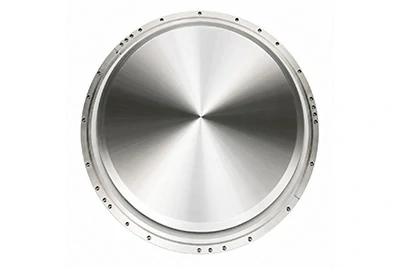
Titanium sputtering targets
Purity:≥5N
Size:8 inch
Grain size:average ≤20 μm, maximum ≤100 μm
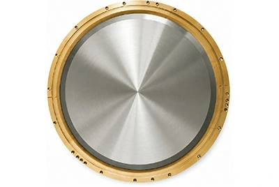
Tantalum sputtering targets
Material:Ta
Purity:≥5N
Grain size:average ≤50 μm, maximum ≤100 μm
Tungsten and tungsten alloy sputtering targets
Materials:W, WTi, WSi
Purity:≥5N
W grain size:average ≤100 μm, maximum ≤200 μm
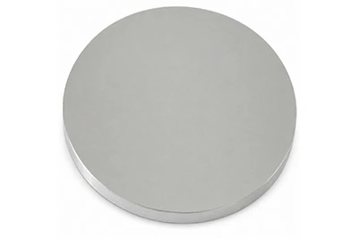

Nickel sputtering targets
Material:Ni
Purity:4N
Size:8 inch
Material: Co
Purity:≥5N
Microstructure:equiaxed or unrecrystallized structure
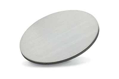
Applications of semiconductor sputtering targets
High-purity metal and alloy sputtering targets can be used for metal thin-film deposition in wafer fabrication, chip packaging, and various semiconductor devices, including interconnect, seed, barrier, and contact layers, electrodes, and backside metallization. For package-level electrical interconnects beyond thin-film deposition, Chalco also supplies die-to-package bonding materials, including semiconductor bonding wire and semiconductor bonding ribbon.
-
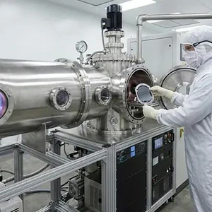 IC wafer fabrication
Used for interconnect, seed, barrier, adhesion, and contact layers, as well as gate metallization in logic chips, memory chips, and other integrated circuits.
-
 Semiconductor and advanced packaging
Used for UBM, RDL, TSV, TGV, bumps, and package-substrate metallization, providing electrical conduction, adhesion, and diffusion barrier functions within chip and package structures.
-
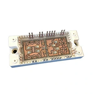 Power semiconductors
Used for front-side electrodes, backside metallization, and contact layers in IGBTs, MOSFETs, power diodes, and power modules to meet high-current and high-temperature operating requirements.
-
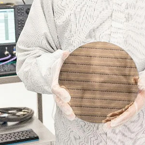 5G RF devices
Used for electrode, conductive-layer, and functional-film deposition in 5G filters, RF front ends, RF chips, and other high-frequency devices.
-
 Third-generation semiconductors
Used for ohmic contacts, electrodes, adhesion layers, barrier layers, and backside metallization in third-generation semiconductor devices such as GaN and SiC devices.
Selecting target materials by film function
Different metal targets offer different characteristics in electrical conductivity, diffusion barrier performance, adhesion, temperature capability, and contact performance. Selection should be based on the target film and device structure.
| Film function | Common target materials | Selection considerations |
| Interconnect and conductive layers | Cu, CuMn, Al, AlCu, AlSi, AlSiCu | Electrical conductivity, alloy composition, and film uniformity |
| Seed layer | Cu, Ti | Film continuity, adhesion, and compatibility with subsequent electroplating |
| Barrier and liner layers | Ta, Ti, WTi | Diffusion barrier performance, interface stability, and temperature capability |
| Adhesion layer | Ti, WTi | Bonding performance with the substrate and overlying metal |
| Contact layers and gates | W, WSi, Co, Ni | Contact resistance, thermal stability, and microstructure |
| Electrodes and backside metallization | Al, AlCu, AlSiCu, Ti, Ni | Electrical conductivity, bondability, and reliability at elevated temperatures |
| UBM and advanced packaging metallization | Cu, Ti, WTi, Ni | Electrical conductivity, adhesion, barrier performance, and thermal cycling stability |
Final selection should also consider the substrate type, deposition temperature, film thickness, PVD equipment, and subsequent processes. Once the target film, equipment model, or existing target drawing is provided, a suitable material system can be matched.
Semiconductor sputtering target forms and structures
Chalco can match monolithic semiconductor sputtering targets or targets with backing plates according to the target material, PVD equipment, operating power, and cooling configuration.
Circular planar targets
Circular planar targets are available for 6, 8, and 12-inch wafer processing systems. Diameter, thickness, hole positions, steps, and mounting interfaces can be machined to drawings.
Monolithic targets
The target is machined as an integral component from a single metal or alloy. This structure is suitable for Cu, CuMn, Al, and some aluminum alloy targets and reduces reliance on a target-to-backing plate bond interface.
Targets with backing plates
The target can be bonded to a backing plate to support installation, cooling, and operational stability. Backing plate material, thickness, and cooling structure are confirmed from the equipment drawing.
Multiple bonding methods
Depending on the material and equipment requirements, EB, SB, FSW, DB, or HIP can be used to bond the target to the backing plate, and C-scan can be used to inspect bond integrity.
Customization by equipment model or existing target part number
Target dimensions, mounting structure, backing plate, and bonding method can be matched to the PVD equipment model, existing target part number, current sample, or customer drawing.
Chalco's customization capabilities for semiconductor sputtering targets
- Material options: Cu, CuMn, Al, AlCu, AlSi, AlSiCu, Ti, Ta, Co, Ni, W, WTi, and WSi target materials are available.
- Purity control: Purity grades are matched to film performance and deposition process requirements, with control of critical impurity elements.
- Alloy composition: The proportions of Mn, Si, Cu, Ti, and other alloying elements can be confirmed based on product specifications and process requirements.
- Dimensions: Common sizes cover 6, 8, and 12 inches. The exact outside diameter, thickness, and structure are confirmed against drawings.
- Grain structure: Grain size, crystallographic orientation, and multiphase microstructure can be controlled according to the material type.
- Target structure: Monolithic targets and target-to-backing plate assemblies are available.
- Bonding method: FSW, DB, HIP, SB, or EB can be selected according to the material and structural requirements.
- Customization basis: The production plan can be determined from target drawings, technical requirements, equipment information, or an existing sample.
After receiving the target material, purity, dimensions, and structural requirements, we can confirm a suitable customization plan and provide a quotation.
Advanced equipment supports consistent target production
From raw material purification and melting and forming to precision machining, bonding, and inspection, a complete equipment setup supports control of semiconductor target purity, microstructure, dimensions, and batch-to-batch consistency.
- Purification and magnetic levitation melting equipment: Used for high-purity metal purification, melting, and alloying to reduce contamination during melting and improve alloy composition uniformity.
- IPAS grain refinement and heat treatment equipment: Controls target grain size, crystallographic orientation, and microstructural uniformity to meet different thin-film deposition process requirements.
- Rolling and isostatic pressing equipment: Improves internal density and microstructural consistency, reducing the risk of pores, inclusions, and localized microstructural variation.
- CNC and precision turning equipment: Machines the target outside diameter, thickness, and mating features. CMM inspection accuracy can reach 0.001 mm, supporting accurate target installation in the equipment.
- FSW and DB bonding equipment: Bonds the target to the backing plate according to the target material and structure, improving the integrity and stability of the bonded area.
- Automated cleaning line: Works with an ultrapure water system for cleaning, drying, and clean processing to reduce particles, oil, and surface residues.
- ICP-MS and XRF: Used to test purity, trace impurities, and alloy composition. ICP-MS detection accuracy can reach 0.001 ppb.
- Electron microscopy and microstructure inspection equipment: Examines grain structure, microstructure, and surface condition, providing data for thermo-mechanical processing and grain control.
- C-scan inspection equipment: Inspects the bonded area of bonded targets to identify unbonded regions, voids, and other internal anomalies.
- Surface roughness testers and vacuum packaging equipment: Control target surface quality and use vacuum packaging to reduce contamination and oxidation risks during storage and transportation.
Chalco semiconductor sputtering target production process
Chalco develops suitable purification, forming, microstructure-control, and precision-machining processes for each metal and alloy target, enabling consistent control of target purity, grain structure, dimensions, and target-to-backing plate bond quality.
Raw material preparation
For copper-target production, high-purity copper for semiconductor targets can be selected according to the required target grade, purity level, and critical impurity limits. For other metal and alloy target systems, Chalco selects raw materials according to the corresponding target grade, purity level, and alloy ratio and defines the required impurity-control conditions.
Melting and forming
Melting, casting, or powder-forming processes matched to the material are used to prepare target blanks, with control of alloy composition, internal density, and microstructural uniformity.
Thermo-mechanical processing and microstructure control
Rolling, heat treatment, and grain refinement processes are used to improve target grain size, crystallographic orientation, and microstructure.
Precision machining
Chalco uses turning, cutting, and CNC precision machining to produce the target outside diameter, thickness, and mounting features so that the dimensions conform to the customer drawing.
Target-to-backing plate bonding
FSW, DB, HIP, SB, or EB is selected according to the target material and structural requirements.
Clean washing
Cleaning, rinsing, and drying remove machining residues, oil, and surface particles, reducing the risk of contamination during installation.
Final inspection
Chalco inspects target purity, chemical composition, grain structure, dimensional accuracy, surface quality, and bond condition.
Vacuum packaging
After inspection, the targets are clean-packed and sealed in double-layer vacuum packaging to reduce oxidation, moisture exposure, and contamination during transportation and storage.
Chalco applies process-wide quality control from raw material selection through final packaging to supply semiconductor sputtering targets with consistent purity, uniform microstructure, and controlled machining accuracy.
Information required for a quotation
To help Chalco quickly confirm the target material, structure, and production plan, please provide the following information with your inquiry:
- Target material: Cu, CuMn, Al, AlCu, AlSi, AlSiCu, Ti, Ta, Co, Ni, W, WTi, or WSi.
- Purity requirements: Target purity grade and impurity elements requiring special control.
- Dimensions: Target outside diameter, thickness, backing plate dimensions, hole positions, and other mounting features.
- Target structure: Monolithic target or target-to-backing plate assembly.
- Bonding method: If specified, indicate FSW, DB, HIP, SB, or EB.
- Microstructure requirements: Grain size, crystallographic orientation, density, or multiphase microstructure requirements.
- Application information: Target film, wafer size, semiconductor device type, and deposition process.
- Equipment information: PVD equipment model, existing target part number, or current target drawing.
- Inspection requirements: Required composition, purity, grain structure, dimensional, or bond-quality inspection items.
- Order quantity: Quantity per order, estimated annual demand, and expected lead time.
After receiving the drawing, existing target specification, or equipment information, Chalco can complete the technical assessment more efficiently and provide a corresponding target solution and quotation.
Semiconductor sputtering target FAQs
What semiconductor target materials can Chalco supply?
Chalco can supply high-purity metal and alloy targets in Cu, CuMn, Al, AlCu, AlSi, AlSiCu, Ti, Ta, Co, Ni, W, WTi, and WSi.
What purity levels are available for semiconductor targets?
Purity levels vary by material and can reach up to 6N. The exact purity and critical impurity control requirements should be confirmed according to the target material and thin-film process.
What common sizes are available?
Available specifications cover 6, 8, and 12 inches. Target outside diameter, thickness, and mounting structure can be confirmed from the customer drawing.
Are monolithic targets and targets with backing plates available?
Yes. Chalco can supply monolithic targets or target-to-backing plate assemblies according to the material and equipment requirements.
How should the target material be selected?
Selection should consider the target film function, substrate, deposition process, PVD equipment, and subsequent processes. After receiving the application information, Chalco can help match the corresponding material.
Can targets be customized to an existing drawing?
Yes. Customers can provide the target drawing, technical requirements, equipment model, or existing target specification to confirm the material, dimensions, microstructure, and structural solution.
What inspections are performed before shipment?
Purity, chemical composition, grain structure, dimensions, surface condition, and target-to-backing plate bond quality can be inspected according to product requirements.
How are the targets packaged?
After cleaning and inspection, the targets are sealed in double-layer vacuum packaging to reduce moisture exposure, oxidation, and external contamination during storage and transportation.