Within Chalco's broader die-to-package bonding materials range, Henan Chalco supports conventional wire-bonded packages and selected advanced IC packaging applications with gold, bare copper, palladium-coated copper (PCC), silver alloy, and selected fine aluminum bonding wires, together with preformed Copper Pillar Pins and Pin Modules for vertical copper interconnects. Based on the package architecture, existing specification, or part drawing, we can help narrow the candidate product range and coordinate technical data, engineering samples, and quotation evaluation.
Conventional IC Fine-Wire Interconnects | Advanced IC Copper Interconnects | Sample and Specification Support
Choose the Interconnect Route by Package Architecture
Wire-Bonded IC Packaging
For QFN, DFN, SOIC, TSSOP, QFP, wire-bond BGA, and selected MEMS and sensor packages, with gold, copper, PCC, silver alloy, and selected fine aluminum bonding wires.
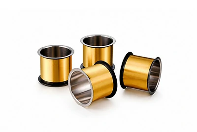
Fine Bonding Wire Solutions for IC Packaging
Advanced IC Packaging
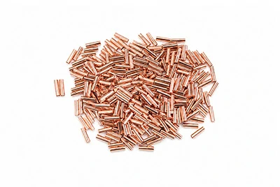
For selected SiP, PMIC, and 2.5D/3D structures, distinguishing the die-side Copper Pillar route from preformed Pillar Pins and Pin Modules.
Advanced IC Packaging Copper Interconnect Solutions
Where Interconnect Products Are Used in IC Packaging
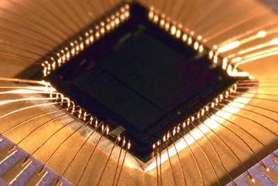
In a conventional wire-bonded IC package, fine bonding wire runs from the die pad to a leadframe terminal or package-substrate pad, providing the electrical connection between the die and the package's external circuitry.
In selected advanced IC packages, Copper Pillar structures provide short vertical connections. A standard Copper Pillar generally refers to a pillar formed on the wafer or die side; a Preformed Copper Pillar Pin is an independently manufactured and delivered micro-interconnect component; and a Pin Module arranges and positions multiple pins as an array or module.
These are not the same product. Before product evaluation, the customer should first determine whether the design requires fine-wire bonding, a wafer-side Copper Pillar structure, or drawing-based preformed pins or pin modules.
Next: Review the product range and selection logic for fine bonding wire in conventional IC packaging.
Fine Bonding Wire Solutions for Wire-Bonded IC Packaging
In QFN, DFN, SOIC, TSSOP, QFP, wire-bond BGA, stacked-die, and selected MEMS and sensor packages, fine bonding wire provides the electrical connection between the die pad and the leadframe or package substrate. Henan Chalco supplies gold, copper, PCC, silver alloy, and selected fine aluminum bonding wires and can help narrow the candidate range based on the incumbent wire, package architecture, and qualification objective.
Common IC Packaging Applications
Leadframe Packages
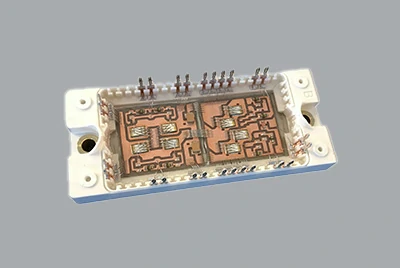
QFN, DFN, SOIC, TSSOP, and QFP typically require bond and loop control within limited pad pitch and package space, while also considering the leadframe finish and the effect of molding on interconnect stability.
Substrate-Based and Stacked-Die Packages
Wire-bond BGA and selected stacked-die packages also require consideration of substrate finish, mixed loop lengths, die-to-die clearance, and loop stability after molding.
Selected Specialty Packages
Some MEMS, sensor, analog, and mixed-signal devices may use ball bonding or fine-wire wedge bonding. Material and tool selection should follow the actual package architecture.
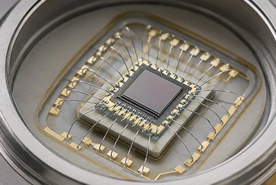
Different package families and applications change the wire, tooling, and validation priorities, so bonding wire should not be selected by device name alone; bonding wire for LED packaging, for example, follows application-specific selection priorities distinct from the IC package architectures discussed here.
Bonding Wire Material Options for IC Packaging
-
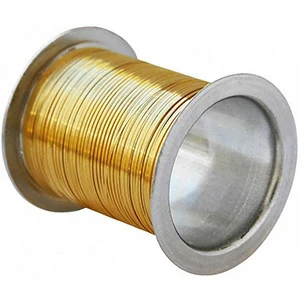 Gold Bonding Wire
Suitable for projects that retain an established gold-wire process, a mature production baseline, or a low tolerance for material-switching risk. Selection should still be aligned with the incumbent wire diameter, mechanical properties, and package requirements.
-
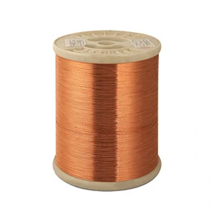 Bare Copper and PCC Bonding Wire
Common candidates for NPI, cost optimization, and second-source evaluation. Introduction should focus on free-air-ball formation, pad-interface behavior, and second-bond performance. PCC is a coated copper-wire option that requires independent evaluation and should not be treated as a direct equivalent to gold or bare copper wire.
-
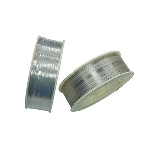 Silver Alloy Bonding Wire
A candidate for selected fine-wire ball-bonding applications. Different alloy or surface systems may produce different ball-formation and bonding responses and should be evaluated against the existing molding system and reliability objectives.
-
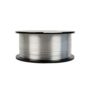 Selected Fine Aluminum Wire
Primarily intended for selected fine-wire wedge-bonded IC, MEMS, or sensor packages. Because the tool and bond geometry differ, it should not be ranked directly against gold, copper, PCC, or silver-alloy ball-bonding wires.
Henan Chalco can use the customer's incumbent product and target package as the baseline for preliminary screening across gold, silver, copper, and aluminum bonding wire systems, rather than relying on a single performance metric or price.
Match Bonding Wire to Existing Package and Process Conditions
After identifying a candidate material, the next step is not immediate replacement of the incumbent wire, but confirmation that it can work with the existing package and equipment conditions. The core review covers four areas:
- Wire: Material system, wire diameter, mechanical properties, and spooling/feed condition;
- Pad and Package: Pad metallization, leadframe or substrate finish, and available package space;
- Bonder and Tool: Ball or wedge bonding, bonder model, and current tool;
- Bond and Loop: First bond, second bond, loop profile, and stability after molding.
Initial discussions can begin with the incumbent wire, package type, and equipment information. Other conditions can be added progressively during sample evaluation. Henan Chalco can then confirm the products, available documentation, and sample range that may be evaluated.
From Candidate Bonding Wire to Approved Supply
NPI, Au-to-Cu/PCC conversion, second-source qualification, and other material changes must be validated in the actual packaging system; wire name or price alone is not sufficient.
- Candidate Review: Compare the existing specification, candidate products, and available technical and quality documentation.
- Sample and Customer Validation: The customer completes bonding, mechanical, and required reliability validation under actual equipment and package conditions.
- Pilot and Approved Supply: Complete pilot production, specification confirmation, approved supply, and subsequent change management in accordance with the customer's process.
Henan Chalco can support technical documentation, engineering samples, and supply coordination. The customer defines the process parameters, acceptance criteria, and package-level qualification.
Vertical Copper Interconnects in Advanced IC Packaging
In selected advanced IC packages, interconnects may be required not only between the die and package substrate, but also between upper and lower package substrates or other stacked package layers. These structures require stable vertical conductive paths within a controlled package height.
Copper Pillars, Preformed Copper Pillar Pins, and Pin Modules differ in how they are formed, where they are used, and the package architectures they support.
-
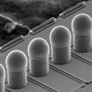 Copper Pillar: Short Vertical Interconnect at the Die Side
A Copper Pillar is typically formed on the wafer or die pad and connects to a package substrate, redistribution layer, or another interconnect layer. It is common in flip-chip, wafer-level packaging, and selected fine-pitch advanced packages.
It is a wafer-level or die-side pillar interconnect that provides a short vertical connection between the die and the underlying package structure; it is not the same as a separately purchased pillar component inserted during package assembly.
-
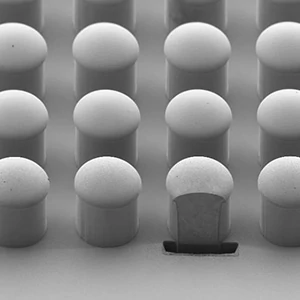 Preformed Copper Pillar Pin: Independent Pillar Component Between Package Layers
A Copper Pillar Pin is a prefabricated micro-pillar manufactured and delivered as an independent component. Round, square, and other custom cross-sections may be evaluated.
In a SiP Module, Copper Pillar Pins can be placed between the upper and lower package substrates to provide vertical electrical connection and maintain the required interlayer height.
In a PMIC Module, Copper Pillar Pins can connect the upper and lower package substrates while reserving space for taller components such as inductors. They are suited to custom designs in which pillar height, pitch, and arrangement are defined by the package architecture.
-
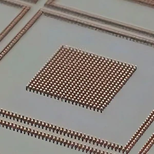 Pin Module: Arrayed Structure for Multi-Point Vertical Connections
When a package requires multiple Pillar Pins at fixed locations, the pins can be pre-arranged to the specified pitch, height, and array layout to form a Pin Module.
Pin Modules can be used in 2.5D/3D SiP and other selected stacked-package structures to create multi-point vertical interconnects between package layers.
The purpose is not to change the function of each pin, but to organize separate pillars into an array or module that matches the package layout and downstream assembly structure.
Typical Package Architectures and Product Forms
| Package Architecture | Location of Copper Interconnect | Closest Product Form |
| Flip-Chip / Wafer-Level Package | From die side to package substrate or RDL | Copper Pillar |
| SiP Module | Between upper and lower package substrates | Preformed Copper Pillar Pins or Pin Module |
| PMIC Module | Between upper and lower package substrates, with clearance for taller components | Preformed Copper Pillar Pins |
| 2.5D / 3D SiP | Interlayer vertical connections at multiple fixed locations | Pin Module |
Henan Chalco focuses on preformed Copper Pillar Pins and Pin Modules. Based on the package architecture and product drawing, we can assess round, square, single-pin, or array-based forms. Material, dimensions, tolerances, surface condition, and delivery format are subject to the confirmed project specification.
Quick Guide to IC Packaging Interconnect Routes and Products
| Package / Architecture | Interconnect Route | Candidate Products or Forms |
| QFN, DFN, SOIC, TSSOP, QFP, Wire-Bond BGA | Fine-wire ball or wedge bonding | Au, Cu, PCC, Ag Alloy, Selected Fine Al Wire |
| Flip-Chip / Wafer-Level Structure | Die-side Copper Pillar interconnect | Copper Pillar route |
| SiP, PMIC, and Selected Stacked Structures | Preformed vertical copper interconnect | Copper Pillar Pins / Pin Modules |
This matrix is intended for preliminary interconnect-route screening. It does not mean that each package family is limited to one interconnect form. Final selection still depends on the package architecture, joining interface, existing process, and customer qualification requirements.
Related metallization materials: Some advanced packaging structures also use RDL, UBM, seed, or barrier layers. Related requirements can be directed to the page for copper, titanium, and aluminum sputtering targets for semiconductor packaging.
IC Packaging Interconnect Supply and Project Coordination
When selecting an IC packaging interconnect supplier, customers evaluate more than a material or individual part. They also need clear product boundaries, alignment between engineering samples and production specifications, traceable lot and change information, and effective coordination when multiple interconnect products are involved in one project.
Henan Chalco can serve as a single project contact for fine bonding wires, preformed Copper Pillar Pins, and Pin Modules, coordinating requirement review, specification confirmation, engineering samples, technical and quality documentation, and commercial communication. Each product category remains supported by its own specialized manufacturing and inspection system.
One Project Window for Multiple Interconnect Products
For customers evaluating Au, Cu, PCC, and silver alloy bonding wires together, or projects that also involve Copper Pillar Pins and Pin Modules, Henan Chalco can receive the package background, current specifications, and commercial requirements through one project window, then confirm the supply scope, documentation, and quotation conditions by product category.
This single project window reduces repeated communication among engineering, quality, and procurement teams. It does not imply that all products come from one production line or use the same qualification method.
Specification, Drawing, and Sample Coordination
Mature production or second-source projects can begin with the incumbent model, approved specification, and sample baseline. New-package or custom Copper Pillar Pin projects can begin with a package cross-section, part drawing, key dimensions, or an existing sample.
Henan Chalco can help review candidate products, available technical documentation, engineering samples, and remaining information gaps, keeping sample specifications, pilot specifications, and subsequent order requirements clearly aligned. A complete process file is not required for the first discussion.
Documentation, Lot Control, and Continuous Supply
Available technical and quality documentation varies by product and may include datasheets, material or coating information, mechanical properties, dimensional or surface inspection results, packaging information, and lot-traceability records.
The required documents, inspection items, and change-control provisions should be defined in the product specification and order terms rather than treated as a fixed package shared by all product systems.
For second-source or material-change projects, attention should also be given to alignment between sample and production specifications, lot identification, agreed inspection, and communication when a confirmed product changes, supporting the transition from engineering evaluation to continuous supply.
The supplier delivers products and agreed documentation to the confirmed specification. The customer defines the final process window, acceptance criteria, and package-level qualification in the actual die, equipment, substrate, and packaging system.
Frequently Asked Questions
We only have the incumbent wire model, not a complete technical specification. Can evaluation begin?
Yes. The incumbent model, wire diameter, material type, package type, and ball- or wedge-bonding process are usually sufficient for preliminary screening. Pad, equipment, tooling, and validation conditions can be added after the candidate product is defined.
How should a second-source or Au-to-Cu/PCC project be evaluated? Can selection be based only on material and price?
No. The current approved baseline should be the starting point. The specific wire's material or coating, mechanical properties, and available documentation should be compared, followed by sample, process, and reliability validation under the existing pad, equipment, and tooling conditions. Process-conversion and qualification costs should also be included in the total implementation cost.
What technical, quality, and traceability documents can be provided?
The document set depends on the product and may include a datasheet, material or coating information, mechanical properties, dimensional or surface inspection results, packaging information, and lot-traceability records. The actual available documents, inspection items, and acceptance basis should be confirmed during quotation or specification review.
Do Non-Stick, Wire Break, or Wire Sweep always indicate a bonding wire problem?
Not necessarily. Pad surface condition, tool condition, equipment parameters, wire feed, loop design, and molding can all affect the result. The failure location, affected lot, and any equipment or process changes should be reviewed together. Henan Chalco can support checks of the product, lot, and agreed inspection records.
Can evaluation begin without a complete Copper Pillar Pin or Pin Module drawing?
Yes. A package cross-section, structural sketch, existing-sample photo, or known key dimensions can be used to start. Once the pin location, approximate height, cross-section, pitch, and array layout are understood, the product form and remaining design information can be identified preliminarily.
Who is responsible for final package-level qualification?
The supplier can provide agreed product documentation, engineering samples, and product-related support. The customer must define the process window and acceptance criteria and complete package-level qualification using the actual die, equipment, substrate, and packaging conditions.
Submit Your IC Packaging Interconnect Requirements
Select Fine Bonding Wire, Copper Pillar Pin, or Pin Module and send the available specification, package architecture, drawing, or sample information. If the information is not yet complete, you can submit what is currently available, and Henan Chalco will help confirm the product scope and the next information required.
Bonding wire project: Incumbent material or model, wire diameter, package type, and ball-bonding or wedge-bonding process.Copper pillar pin project: Package architecture or drawing, pin location, height or cross-section, pitch, and array layout.