Precision copper pillars and copper blocks are solderable, discrete interconnect components for SiP and 3D packaging, with cylindrical diameters from Φ0.09–2 mm and heights up to 6 mm.
They are a different product category from Cu pillar bumps formed by wafer-level electroplating — this page covers discrete precision components mounted by SMT and reflow soldering.
Henan Chalco supplies both cylindrical and square form factors to drawing / to specification, with bare copper or gold-plated surface finishes, shipped by tape and reel or in bottles.
What Is a Copper Pillar? Discrete Pillar Pins and Plated Pillar Bumps Explained
Within broader IC packaging interconnect solutions, copper pillar is an umbrella term for columnar copper interconnect structures used in advanced packaging.
Depending on the manufacturing method and package position, our copper pillar products fall into two main product forms:
Copper Pillar Pin (Discrete, SMT-Mounted)
Precision-machined, discrete copper pillar and copper block components, mounted between substrates by standard SMT placement and reflow soldering.
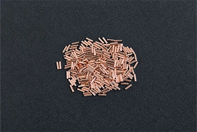
Copper Pillar Pins are used for vertical interconnect, support and EMI shielding in SiP and PMIC modules.
Dimensional precision comes from machining rather than plated growth, with heights from sub-millimeter to several millimeters, decoupled from diameter.
Henan Chalco offers ready supply across ten standard size grades from Φ0.09–2 mm; specifications, materials and applications are detailed below.
Copper Pillar Bump (Wafer-Level Electroplated)
A bump structure formed by electroplating through a photolithographically opened window on a wafer pad, typically topped with a lead-free solder cap.
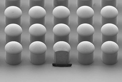
Copper Pillar Bump is used for fine-pitch flip-chip interconnects, with pitches down to tens of micrometers and heights typically ranging from tens of micrometers to about 200 µm (set by plating time and process window), widely used in high-I/O-density packages such as processors and HBM.
Henan Chalco can source copper pillar bump capacity to your wafer-level packaging specification — process node, pitch, material stack and production capacity are confirmed per project.
The specifications, materials and applications below cover Copper Pillar Pin. For wafer-level electroplated copper pillar bump solutions, please specify your process node and pitch requirements in your RFQ, and we will source resources on a per-project basis.
Copper pillar and copper block specifications
Standard specifications cover ten cylindrical diameter grades and six square cross-section grades.
Sizes beyond the ranges below are quoted to drawing (custom sizes are quoted to drawing) — including diameters finer than Φ0.09 mm and square cross-sections larger than the standard grades, both available as custom items;
Send your pad layout and pitch requirements for a feasibility review.
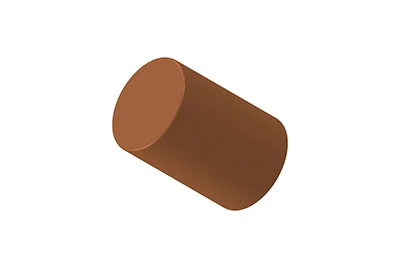
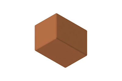
Cylindrical copper pillars
| Type | Diameter (Φ) | Pad pitch | Height range (mm) | Dia. tolerance (mm) | Length tolerance (mm) |
| Cylinder | Φ2 mm | >2.2 mm | 0.65–3.0 | ±0.015 | ±0.020 |
| Cylinder | Φ1.5 mm | >1.7 mm | 0.65–3.0 | ±0.015 | ±0.020 |
| Cylinder | Φ1 mm | >1.2 mm | 0.80–6.0 | ±0.015 | ±0.020 |
| Cylinder | Φ0.8 mm | >1 mm | 0.65–6.0 | ±0.015 | ±0.020 |
| Cylinder | Φ0.4 mm | 500–600 µm | 0.26–6.0 | ±0.010 | ±0.015 |
| Cylinder | Φ0.25 mm | 350–500 µm | 0.16–5.0 | ±0.010 | ±0.015 |
| Cylinder | Φ0.2 mm | 300–400 µm | 0.13–5.0 | ±0.010 | ±0.015 |
| Cylinder | Φ0.15 mm | 275–350 µm | 0.10–1.0 | ±0.010 | ±0.015 |
| Cylinder | Φ0.12 mm | 220–300 µm | 0.08–1.0 | ±0.010 | ±0.015 |
| Cylinder | Φ0.09 mm | 150–220 µm | 0.08–1.0 | ±0.010 | ±0.015 |
Square copper blocks
| Type | Cross-section (W×T) | Length range (mm) | Tolerance (mm) |
| Square | W0.2 × T0.2 mm | 0.2–1.0 | ±0.015 |
| Square | W0.23 × T0.33 mm | 0.33–1.0 | ±0.015 |
| Square | W0.4 × T0.33 mm | 0.4–1.0 | ±0.015 |
| Square | W0.4 × T0.4 mm | 0.4+ | ±0.015 |
| Square | W0.35 × T0.35 mm | 0.35+ | ±0.015 |
| Square | W0.3 × T0.7 mm | 0.7+ | ±0.015 |
Both cylindrical (round) and square form factors are available with bare copper or gold-plated surface finishes.
Need a size outside these ranges?
Custom dimensions are quoted to your drawing — send your drawing for evaluation.

Copper alloy options: conductivity, thermal performance and CTE
| Code | Composition | CTE (10⁻⁶/K) | Thermal conductivity (W/mK) | Conductivity (%IACS) | Specific gravity |
| C8 | Cu + Zn 0.2% + Mg 0.15% | 17.5 | 300–330 | 76–83 | 8.9 |
| C9 | Cu + Sn 0.15% | 17.3 | 360 | 82 | 8.9 |
| CB | Cu 99.99% | 17.7 | 391 | >99 | 8.9 |
| AC | Cu >99.99% | 16.3 | >400 | >100 | 8.92 |
| C5191 phosphor bronze(shown for comparison) | Cu + Sn 5.5–7.0% + P 0.03–0.35% | 18 | 65 | 14 | 8.84 |
How to choose:
The CB and AC high-purity copper grades target current-carrying and heat-dissipation-priority scenarios — power paths, PMIC modules, and designs that also use the pillar as a thermal path — with conductivity >99 %IACS and thermal conductivity of 391–400+ W/mK.
C8 and C9 micro-alloyed copper grades combine high conductivity (76–83 %IACS) with improved strength and processability, suited to structural positions that require component rigidity.
C5191 phosphor bronze, a common pin-type copper alloy, is not well suited to high-current, high-heat scenarios: its thermal conductivity of 65 W/mK and conductivity of 14 %IACS trail high-purity copper by several times to an order of magnitude.
A higher %IACS means lower resistance — less heat generated under current, more efficient heat conduction through the pillar, lower EMI noise from current crowding, and less attenuation and delay for high-frequency signals.
Copper pillars vs solder balls, cu core balls and through mold vias
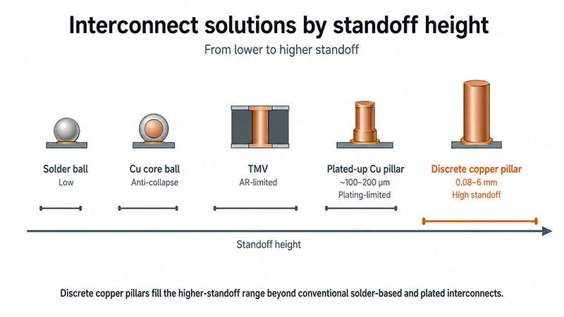
The first differentiating variable among vertical interconnect options is standoff height.
The table below also lists Copper Pillar Bump as a reference dimension, to help you decide which product line to pursue and which product to source.
| Option | Height capability | Height–diameter coupling | Process route | Electrical & thermal cross-section | Typical use point |
| Solder ball | Post-reflow ball height, up to about 300 µm | Height strongly coupled to ball diameter, further reduced by reflow collapse | Ball placement + reflow, a mature process | Solder cross-section, moderate electrical and thermal performance | BGA, standard-pitch interconnects |
| Cu core ball | Copper core does not melt during reflow, helps maintain standoff and resist collapse | Height still capped by ball diameter | Compatible with ball-placement processes | Copper core + solder shell | Stacked interconnects requiring collapse resistance |
| Through mold via (TMV) | Via formed in the mold, depth constrained by aspect ratio | Deeper vias require larger diameters; cost rises with depth | Laser drilling + via fill, an in-house OSAT process | Filled conductor cross-section | PoP mold-embedded conduction |
| Plated-up copper pillar (wafer-level electroplating) | On the order of 100–200 µm, height limited by deposition time | Height set by plating time; plated thickness prone to variation | Photolithography + electroplating, a wafer-level process | Electroplated copper cross-section | Fine-pitch flip-chip interconnects |
| Discrete copper pillar | 0.08–6 mm, height independent of diameter | No coupling — fine diameters can still form tall pillars (high aspect ratio) | SMT placement + reflow | Solid copper cross-section, strong electrical and thermal performance | High standoff, board-to-board stacking, shielding walls |
When the required standoff exceeds what a reflowed solder ball can maintain, when a Cu core ball's diameter tops out, or when TMV aspect ratio and cost are no longer practical, discrete copper pillars are designed to provide freedom in height — height is set by cut length and decoupled from diameter;
Dimensional precision comes from machining (see the specification tables for tolerances) rather than plating growth time — revising the interlayer height only requires a different cut length, with no need to requalify a plating process window.
Conversely, for fine-pitch, low-height interconnects, solder balls and electroplated bumps remain a mature and reasonable choice; copper pillars are not a universal replacement, but fill in the "taller" end of the capability range.
Applications in SiP, PMIC modules and 3D packaging
SiP board-to-board support and conduction
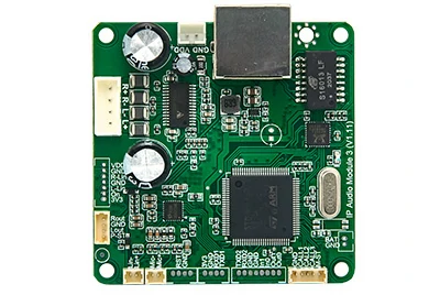
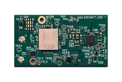
In SiP modules, cylindrical copper pillars are placed between the main board and the bottom substrate, handling three roles at once: mechanical support, electrical conduction, and a heat-dissipation path — the solid copper cross-section combines the current path and the heat path in the same pillar, delivering both high conductivity and high heat dissipation.
The columnar shape is also more transfer-mold friendly: molding compound flows smoothly between pillars, helping reduce fill defects.
EMI compartment shielding with copper blocks
Square copper blocks (copper block / metal bar) act as internal partition walls within a module: connecting the top metal shield to the substrate ground structure and dividing the package interior into shielded compartments (compartment shielding) that isolate digital circuitry from RF/analog interference.
Metal-wall shielding approaches have been described as simple to assemble with good shielding effectiveness at lower frequencies. Unlike stamped shielding frames that require tooling, square copper blocks need no mold and are placed by standard SMT — revising the partition layout only requires adjusting the placement program.
High aspect ratio standoffs in PMIC modules
PMIC modules often need to accommodate tall components such as inductors between the upper and lower substrates.
High-aspect-ratio copper pillars use a small diameter to create several millimeters of interlayer height, freeing up space for bulky components — a geometry that ball-based approaches cannot achieve: a ball tall enough must also be thick enough.
Mixed sizes in 3D packaging
In the multi-layer stacks of 3D packaging, different sizes can be mixed within the same package: small-diameter copper pillars between upper dies, larger-diameter copper pillars between the bottom substrates, with each layer matched to pillars sized for its own gap.
Ten standard diameter grades allow this mixing without developing new components layer by layer.
Mounting and assembly: SMT placement, reflow and tape-and-reel supply
Discrete copper pillars go through a standard surface-mount flow: solder printing → SMT pick and place → reflow.
In module-stacking applications, the subsequent molding and grinding steps (grinding exposes the pillar end faces) are equally compatible — pillars remain coplanar at the end face after molding and grinding, ready for the next interconnect layer.
Packaging is available as tape and reel or in bottles, suited to automated feeding and small-batch trial production respectively.
For high-volume scenarios with hundreds to thousands of pillars per board, options beyond individual placement include using alignment fixtures or a pin insertion mask, combined with vibration or air feeding, to align and place large quantities of pillars in one pass on a solder-paste-printed substrate.
Appearance and dimensional consistency within a batch helps maintain stable placement yield — this is the point of the ±0.010–0.015 mm diameter tolerance: the pick-and-place nozzle and vision system are looking at the same component, ten thousand times over.
Quality, consistency and documentation
Dimensional precision is the core quality commitment for these components: cylindrical diameter tolerance of ±0.010–0.015 mm and length tolerance of ±0.015–0.020 mm (see the specification tables), and square cross-section tolerance of ±0.015 mm. Batch consistency is controlled on both appearance and dimension.
The quality management system is certified to ISO 9001 and ISO 14001 (system-level certification).
The specific configuration of compliance and accompanying documentation (RoHS / REACH declarations, certificate of conformance, batch traceability) can be reviewed with your RFQ.
Supply options, customization and RFQ boundaries
Supply basis
Standard sizes are supplied per the two tables above; sizes beyond these ranges — including finer diameters and larger square cross-sections — are quoted to drawing / to specification, with material selectable across the C8 / C9 / CB / AC grades.
Surface finish and packaging
Bare copper or gold-plated surface finish; tape and reel or bottle packaging.
Documentation framework
Orders can be quoted with certificate of conformance and dimensional inspection data as specified in your RFQ — documentation is configured to your RFQ requirements.
Related products
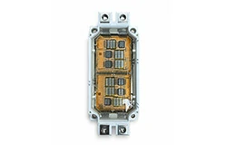
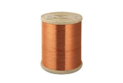
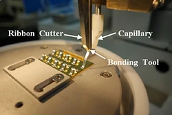
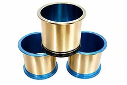
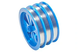
Chalco provides one-stop supply of semiconductor packaging materials, including pin modules, copper bonding wire, power semiconductor bonding wire and ribbon, gold bonding wire, aluminum bonding wire and silver alloy bonding wire.
Pin Module
Frequently asked questions
Is a discrete copper pillar the same as a Cu pillar bump?
No. Both belong to the Copper Pillar product family, in two different forms: Pin is mounted by SMT for board-to-board and in-package interconnects in SiP/PMIC modules; Bump is formed by electroplating on a wafer pad for fine-pitch flip-chip interconnects.
Henan Chalco supplies standard Pin sizes from stock; Bump solutions are sourced on a per-project basis.
When should I use copper pillars instead of solder balls?
When the required standoff height exceeds what a reflowed solder ball can maintain. Solder ball height is coupled to ball diameter and collapses after reflow; pillar height is independent of diameter, up to 6 mm.
What sizes are available?
Cylinders span ten grades from Φ0.09–2 mm, with heights of 0.08–6 mm; square cross-sections span six grades starting from W0.2 × T0.2 mm. Diameters finer than Φ0.09 mm and larger square cross-sections can be evaluated as custom items, quoted to drawing.
How are copper pillars mounted?
Standard SMT process: solder printing, pick and place, reflow. Subsequent molding and grinding processes are compatible.
What materials are offered?
Four copper grades: micro-alloyed C8 / C9 and high-purity CB / AC, with conductivity up to >100 %IACS and thermal conductivity up to >400 W/mK.
Does Henan Chalco supply copper pillar bumps for wafer-level packaging?
Yes. Copper pillar bump solutions can be sourced to your process node, pitch and material system; specific specifications, capacity and minimum order quantity are confirmed through your RFQ.
Can copper blocks be used for EMI shielding inside a package?
Yes. Square copper blocks serve as compartment shielding walls, connecting the metal shield to the ground structure and dividing the module interior into isolated shielded compartments.
Request a quote
Send your drawing or specification for evaluation and a quotation.
To speed up your quotation, please include the following with your RFQ:
- Diameter or cross-section and height
- Tolerance requirement
- Material code or conductivity requirement
- Surface finish
- Quantity and packaging format (tape and reel or bottle)
- Application context (SiP / PMIC / 3D stacking / shielding)
Henan Chalco reviews and supplies to your drawing and specification, quoted to your requirement.